Tom Wada, Prof of the University of the Ryukyus, Information Engineering Dept.
This year's design target is the SybBytes transform circuit, which is one of the key data transformation used in ADVANCED ENCRYPTION STANDARD (AES).
AES encrypts information by repeatedly using the following four kinds of data transformation, ShiftRows, SubBytes, MixColumns, AddRoundKey. The standard document is available in the following URL.
http://csrc.nist.gov/publications/fips/fips197/fips-197.pdf
Since this contest is mainly for University students, the code size in the task is relatively small to let student to design easily. Then the design target is not entire AES encryption /decryption system. The design target is just SubBytes transform circuit. The required function is simple such as the transformation from 8bit data to 8bit data. Then the transformation can be implemented using 256 word x 8 bit Read Only Memory (ROM). However, since the SybBytes transform algorithm is based on Galois Field Inverse operation and simple affine transformation, the function can be realized by small low-power digital circuit once good algorithm is applied for the design.
The requirements of the design is to write HDL (VHDL or Verilog HDL) and to synthesize digital circuits using Synopsys design analyzer or any other EDA tools. Making FPGA is also optional but our judges love to see your FPGA designs.
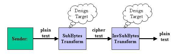
Figure1 System Diagram
The figure 1 shows the system diagram. The system is divided into three blocks such as Sender, SubBytes Transform, and Inverse SubBytes Transform. Sender generates 1 byte (8 bit) data serially. SubBytes Transform encipher the 8bit. Inverse SubBytes Transform decipher the encrypted 8bit to plain byte. The design target is the transform circuit which can both execute SubBytes and Inverse SubBytes transformations by mode switch signal.
SubBytes transform is a simple transform which converts 8bit data to other 8 bit data. For example, 8 bit data "00000000" is transformed into "01100011". What is important is that different byte data are always transformed into different 8 bit data. If this condition is violated, the transformed data can not be recovered. Such system can not be used for data encryption. This required condition does fit Galois Field characteristics.
The definition of SubBytes Transformation is the serial transformation of the following two transformation.
- Take the multiplicative inverse in Galois Field GF(28), the element 8bit "00000000" = hex {00} is mapped to itself.
Inverse Table is shown as follows. For example, 8bit number "01010011" is {53} in hexadecimal. Then consult table by X=5, Y=3, then the output {CA} in hex is obtained. {CA} is "11001010" in binary format.
Y
0 1 2 3 4 5 6 7 8 9 A B C D E F X 0 00 01 8D F6 CB 52 7B D1 E8 4F 29 C0 B0 E1 E5 C7 1 74 B4 AA 4B 99 2B 60 5F 58 3F FD CC FF 40 EE B2 2 3A 6E 5A F1 55 4D A8 C9 C1 0A 98 15 30 44 A2 C2 3 2C 45 92 6C F3 39 66 42 F2 35 20 6F 77 BB 59 19 4 1D FE 37 67 2D 31 F5 69 A7 64 AB 13 54 25 E9 09 5 ED 5C 05 CA 4C 24 87 BF 18 3E 22 F0 51 EC 61 17 6 16 5E AF D3 49 A6 36 43 F4 47 91 DF 33 93 21 3B 7 79 B7 97 85 10 B5 BA 3C B6 70 D0 06 A1 FA 81 82 8 83 7E 7F 80 96 73 BE 56 9B 9E 95 D9 F7 02 B9 A4 9 DE 6A 32 6D D8 8A 84 72 2A 14 9F 88 F9 DC 89 9A A FB 7C 2E C3 8F B8 65 48 26 C8 12 4A CE E7 D2 62 B 0C E0 1F EF 11 75 78 71 A5 8E 76 3D BD BC 86 57 C 0B 28 2F A3 DA D4 E4 0F A9 27 53 04 1B FC AC E6 D 7A 07 AE 63 C5 DB E2 EA 94 8B C4 D5 9D F8 90 6B E B1 0D D6 EB C6 0E CF AD 08 4E D7 E3 5D 50 1E B3 F 5B 23 38 34 68 46 03 8C DD 9C 7D A0 CD 1A 41 1C Table 1. multiplicative inverse table in GF(28)
Irreducible polynomial is as follows.
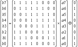
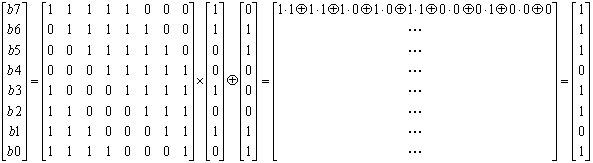
- Then apply the affine transformation over GF(2). Binary "00000000" = Hex {00} will be transformed into "01100011"={63}.
If (a7, a6, a5, a4, a3, a2, a1, a0)={CA}, then the computation over GF(2) is performed as follows.
{CA} will be transformed into "11101101 ={ED}.
Totally, {53} is converted to {CA} by Inversion, and then transformed into {ED} by affine transform. These serial transform is SubBytes transformation.
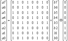
Inverse SubBytes Transformation is the reverse operation of SubBytes transformation. Then the following two serial transformation will be executed.
- The inverse affine transformation is executed. The inverse transformation will be given in the following equation.
- Then perform the same multiplicative inverse in Galois Field GF(28) according to the table 1.
Since both SubBytes and Inverse SubBytes transformations needs the multiplicative inverse in Galois Field GF(28), the design target function can be realized in the architecture shown in figure 2.
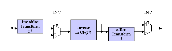
Figure 2. Architecture Example
When INV signal is '0', input data first goes to Inverse Block then transferred to affine transform, and when INV signal is asserted (='1'), input data is first transformed in Inv Affin Block and later Inverse in GF(28) is caluculated.
Since the affine transform is just a calculation using ANDs and EXORs, how calculate the inverse in GF(28) should be weill considered in the design task.
Most easy implementation of Inverse calculation in GF(28) is to use 256 word x 8 bit ROM which possesses the data in Table 1.
However, the ROM implementation is not intersting in the design contest.
Another implementation idea will be explained as follows.
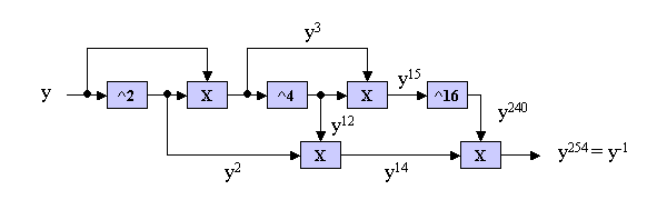
Suppose input is y in GF(28) , y-1 has to be calculated. In G(28) ,
is satisfied. Then,
Consequently, y254 is equivalent to y-1. Figure 3 shows an Inversion circuit based on Itoh and Tsujii's algorithm.
Figure 3. An Inversion circuit based on Itoh and Tsujii's algorithm
According to the preceding section, inverse can be computed by the repetitive use of multiply circuits.
Suppose the multiply of two 8-bit value A= (a7, a6, a5, a4, a3, a2, a1, a0), B=(b7, b6, b5, b4, b3, b2, b1, b0). Since those 8 bit value can be expressed in polynomials in Galois Field such as
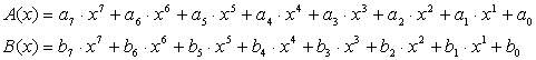
Then C(x) = A(x) * B(x) gives
The result is 14th order polynomials. Be sure to remember that all coefficients follows GF(2) rule. Then multiply is replaced withs AND logic, addition/subtraction are replaced with exclusive-or logics.
Assuming Irreducible polynomial = 0, the following relations are obtained.
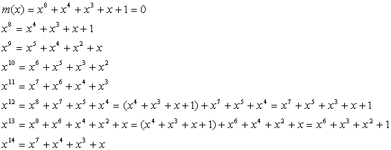
By applying those relations to C(x), C(x) can be modified into 7th order polynomial D(x).
Since D(x) expresses GF(28) , the multiplication result of two numbers in GF(28) A= (a7, a6, a5, a4, a3, a2, a1, a0)、B=(b7, b6, b5, b4, b3, b2, b1, b0) will be D=(d7, d6, d5, d4, d3, d2, d1, d0) .
In another words, multiplication in GF(28) can be implemented using AND and EXOR logics.
(NOTE) The above equation is not fully debugged. If you use the equation, please check by yourself.
The beginners' task has the following pin lists.
|
SubBytes |
|||
| signal name | in or out | bit width | explanation |
| CLK | IN | 1 | clock input |
| RESET | IN | 1 | assertion '1' means reset |
| XIN | IN | 8 | input data |
| INV | IN | 1 | '0' means SubBytes, '1' means Inverse SubBytes |
| YOUT | OUT | 8 | transformed output |
Table 2. Pin list for LEVEL1
SENDER, SUBBYTES (usign ROM, INV function is not supported) and TESTBENCH VHDL file is linked as follow. Please use as it is or modified.
SENDER: sender.vhd
SUBBYTES TRANSFORM: subbytes.vhd
TESTBENCH: test_subbytes.vhd
Figure 4 shows the simulated waveform.
SENDER generates 8 bit input signal.
SUBBYTES output is generated with 2 cycle delaye.
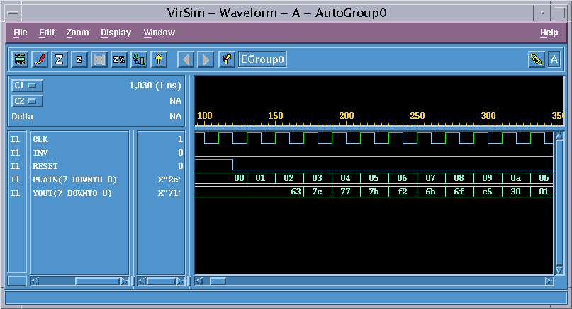
Figure 4. Simulation Waveform
In the Level 2 task, you do NOT need to follow the detail design spec.
Mandatory rule is
1) Please design circuit which can perform both SubByes and Inverse SubBytes Transform.
2) Any Architecture, any timing, any pin list are acceptable. I believe you can enjoy your originality.
Since it is impossible to use the same synthesis library for various participants, use the 1 exor gate delay as a unit for speed comparison.
In the previous example, total delay = 7.17 ns and 6 circuit stages, then the 7.17/6= 1.195 ns is the unit of the speed. Please normalize your circuit speed by this unit.
| Title page | 1 | Team name, Members Name, School, Grade |
| 2 | Address, Phone, Email-address | |
| 3 | T-shirt size for all members in the team | |
| 4 | Which level of task is designed. | |
| Contents | 1 | Circuit block or architecture description |
| 2 | Designed circuit functional explanation, etc. | |
| 3 | Appealing point and originality | |
| 4 | Critical path speed, and circuit area | |
| 5 | HDL codes (VHDL or Verilog HDL) | |
| 6 | Simulation waveform indicating the design is operating! | |
| 7 | Anything you want to claim |
Report has to be emailed to the following address. Please use PDF file format.
If you want to send the report data other than PDF, please consult me.
This program is
operated by Univ. of Ryukyus, IE dept.,
co-operated by Okinawa Industry Support Center,
and co-sponsored by SONY LSI Design Inc.
ENJOY HDL! We want to see you at OKINAWA!