Tom Wada, Prof of the University of the Ryukyus, Information Engineering Dept.
Last year, we have designed All Digital FM Receiver Circuit as the contest design task. However, the real digital communication system requires error correction capability. Recently, very high performance error correction methods approaching to the Shannon Limit are utilized in the real applications such as TURBO codes and LDPC (Low Density Parity Check) codes. Those error correction decodes uses Iterative processing.
Since this contest is mainly for University students, we try to realize the target design as simple as possible. This year's design task is "2-D product code Iterative Decoder". Every 4 bits transmitting data is arranged in 2X2 matrix form in the transmitter. The transmitter also generates 2 row parity bits and 2 column parity bits. Then, 4bit data and 4 bit parity form one processing data packet. The 8 bits in the packet is modulated by BPSK (Binary Phase Shift Keying). Those BPSK modulated data is transmitted. In the transmission channel, Noise will be added. At the receiver side, error correction processing will be performed. One typical decoder architecture is to use Iterative processing.
The requirements of the design is to write HDL (VHDL or Verilog HDL) and to synthesize digital circuits using Synopsys design analyzer or any other EDA tools. Making FPGA is also optional but our judges love to see your FPGA designs.
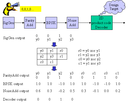
Figure1 System Diagram
Figure 1 shows the 2D product code transmission system. Transmitting Information Generator (SigGen) generates binary signals (See y0, y1, y2, y3). ParityAdd block adds 4 bits parity bits such as r0, r1, c0, c1 to the 4 bits SigGen outputs as y0, y1, y2, y3. In the BPSK processing block, those binary information are modulated. The binary information 0 and 1 is modulated to 1.0 and -1.0 respectively. The Noise Add block adds random noise to the BPSK signals. Finally, the design task of "2-D product code decoder" performs error correction operation and outputs the error corrected binary bits.
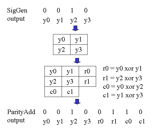
Figure 2-D Product Code
Figure 2 again shows the generation of the 2-D Product code. The 4 bits of SigGen outputs are grouped as {y0, y1, y2, y3}. Those 4 bits form 2X2 matrix as shown in the figure. Then the row parity bits r0, r1 and column parity bits c0, c1 is calculated by the equation in the figure. Then total 8bits {y0, y1, y2, y3, r0, r1, c0, c1} are generated as 2-D Product Code. Since information bit is 4 and total bit is 8, then code rate is defined as R (code rate) = 1/2 = (information bits) / (code total bits).
When you want to send 0 or 1 binary data by wireless, you have to use radio wave signal. The BPSK modulation is to use two different phase (0 degree and 180 degree) sinusoidal wave. Detail BPSK explanation is not give here. But, 1.0 means phase= 0 degree cosine wave and -1.0 means phase = 180 degree cosine wave, since cos(0 degree) = 1.0 and cos(180 degree) = -1.0. In the figure 3, you can see this BPSK modulation. Since the mid point of the BPSK output is 0.0, at the receiver side if the received signal is positive, the receiver demodulate output will be "0" information and if the received signal is negative, the demodulated output will be "1" information.
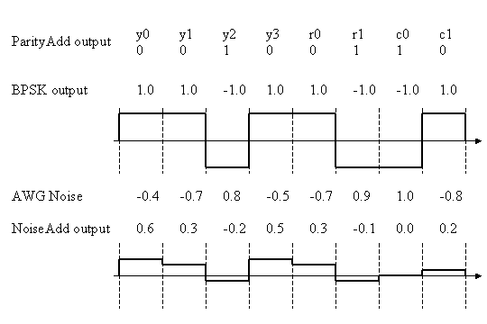
Figure 3 BPSK modulation and Noise Addition
This BPSK modulated signal is transmitted by the radio wave and Noise will be added. We are going to assume that the Noise is White Gaussian Noise. Then the noise voltage avarage in long time should be 0.0 and the distribution of the Noise voltage obey the Gaussian distribution.
Signal to Noise power ration (SNR) is defined by the power ratio between signal and noise. In the BPSK case as shown in the figure 3, the signal power avarage is 1.0 since the voltage swing is 1.0 or -1.0.
The noise power average in figure 3 is calculated as follows.
Noise Power= 1/8*(0.16 + 0.49 + 0.64 + 0.25 + 0.49 + 0.81 + 1.0 + 0.64)=0.56
Then, SNR = 1.0/0.56 = 1.78.
Usually, dB value is used then
SNR (in dB) = 10*log10(1.78) = 2.5dB.
Therefore, the figure 3 case is adding 2.5dB noise. The bottom wave is actual received wave form including the noise power.
(3-1) priori probability and posteriori probability
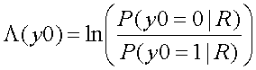
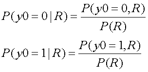
2-D product code decoder gets 8 received signals R={Ry0, Ry1, Ry2, Ry3, Rr0, Rr1, Rc0, Rc1} and then estimate original 4 bit information {y0, y1, y2, y3}. Since y0 could be "0" or "1", we have to compare the following two probabilities.
1) probability of sending information y0="0" when we received R={Ry0, Ry1, Ry2, Ry3, Rr0, Rr1, Rc0, Rc1}
![]()
2) probability of sending information y0="1" when we received R={Ry0, Ry1, Ry2, Ry3, Rr0, Rr1, Rc0, Rc1}
![]()
Before receiving R signals, the probability P(y0=0) = P(y0=1) = 0.5.
However, after receiving R, the probability P(y0=0 | R) and P(y0=1 | R) may be different. The probability P(y0=0) or P(y0=1) before receiving R is called as priori probability and P(y0=0 | R) and P(y0=1 | R) after receiving R is called as posteriori probability.
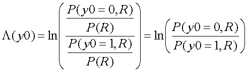
(3-2) log posteriori probability ratio (posteriori value)
In order to compare the two posteriori probability, log posteriori probability ratio (posteriori value Λ ) is defined as follows.
Using the posteriori value, the magnitude of the two probability comparison will be judged by the sign (plus or minus) of the posteriori value Λ.
According to the Basian low,
Then,
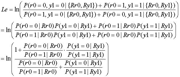
(3-3) postrioti value = channel value + priori value + external value
The meaning of P(y0=0,R) is the probability in the case of the sending information y0=0 and the received signal R={Ry0, Ry1, Ry2, Ry3, Rr0, Rr1, Rc0, Rc1}.
The parity equation r0=y0 xor y1 is transfomed into y0=r0 xor y1. Therefore, if y0=0 then r0 xor y1=0. Then the posteriori value Λ can be transformed as follows.

Then,
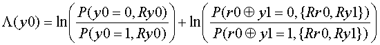
Use Basian low to the 1st term.

Finaly,

This final equation means as follows
1) The 1st term is the log probability ratio between the probability of receiving Ry0 when sending y0=0 and the probability of receiving Ry0 when sending y0=1. This value is determined by the Noise at the transmission channel. Then we call this term as Channel Value Lch.
2) The 2nd term is the log probability ratio between the probability of sending y0=0 and the probability of sending y0=1. This value is determined by the transmitter. Then we call this value as Priori Value Lpri.
3) The 3rd term is the log probability ratio relating to the parity bits, not relating to y0 itself. Then we call this term as External Value Le.
Then Posteriori Value Lpost can be expressed as follows.
Lpost = Lch + Lpri + Le.
(3-4) Lch value calculation when BPSK modulation is used and Noise is AWGN
When Additive White Gaussian Noise (AWGN) is added to the BPSK modulation signal, the received signal value will be dispersed at the center of 1.0 or -1.0. The distribution follows the Gaussian Distribution as shown in the figure 4.
The distribution function is as follows.
1) if sending signal is 1.0,
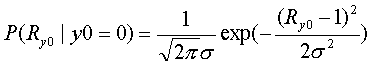
2) if sending signal is -1.0,
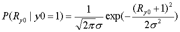
Here, σ2 is Variance which is the square of standard deviation.
Then, the Channel Value Lch is as follows.
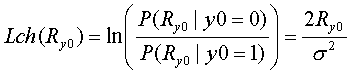
Finally, Lch is proportional to the received signal value Ry0.
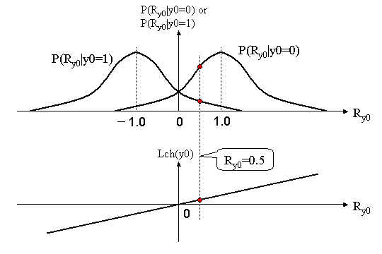
Figure 4 The deviation of BPSK received signal with AWGN and Channel Value Lch
(3-4) External Value Le calculation
As shown in (3-3), the external value Le can be calculated as follows.
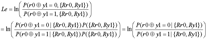
If r0 xor y1=0, then r0=y1=0 or r0=y1=1. If r0 xor y1=1, then r0=0, y1=1 or r0=1, y1=0. Then the Le can transformed as follows.
Here, we define Λr0 and Λy1 as follows.
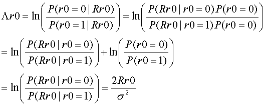
When the magnitudes of |Λr0|, |Λy1| have large diffference, Le can be approximated as follows.
Sgn(a * b) means the sign of a*b. If a*b is possitive, sgn(a*b) means 1.0. If a*b is negative, sgn(a*b) means -1.0.
Min(|a|, |b|) returns the value of the smaller one of absolute of a or absolute of b.
In the following, circuit implementation example, this approximation will be used.
In the section [3], the algorithm equation is explained. In this section, more detail decoding processing will be explained.
STEP1: Receive 8 real values R={Ry0, Ry1, Ry2, Ry3, Rr0, Rr1, Rc0, Rc1}
In the following calculation, we need to use 2/σ2 to get Lch value. However, The magnitude of 2/σ2 does not effect of the sign of the Lpost value. Then, in the following calculation 2/σ2 = 1 is assumed. Then Lch values are the same as {Ry0, Ry1, Ry2, Ry3, Rr0, Rr1, Rc0, Rc1}.
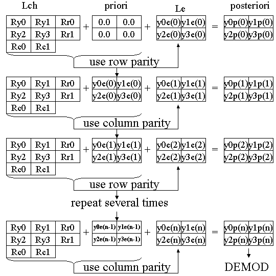
Figure 5 Iterative Decoding Process
STEP2: External Value Le calculation
As shown in the top in the figure 5, Lch and priori are added. In the first step, priori values are all 0.0. Le is calculated from this added result. The Le computation can be done by either row parity equation and column parity equation. However, just we choose row parity equation for the 1st iteration as follows.
y0e(0) = sgn(Ry1*Rr0) * min(|Ry1|, |Rr0|)
y1e(0) = sgn(Ry0*Rr0) * min(|Ry0|, |Rr0|)
y2e(0) = sgn(Ry3*Rr1) * min(|Ry3|, |Rr1|)
y3e(0) = sgn(Ry2*Rr1) * min(|Ry2|, |Rr1|)
This computed Le will be used next step priori value.
STEP 3: Next Le calculation by using the 1st Le as priori value and column parity equation
As shown in the second from the top in the figure 5, next Le is computed as follows. Column parity is used.
y0e(1) = sgn( (Ry2+y2e(0)) * Rc0 ) * min(|Ry2+y2e(0)|, |Rc0|)
y1e(1) = sgn( (Ry3+y3e(0)) * Rc1) * min(|Ry3+y3e(0)|, |Rc1|)
y2e(1) = sgn( (Ry0+y0e(0)) * Rc0 ) * min(|Ry0+y0e(0)|, |Rc0|)
y3e(1) = sgn( (Ry1+y1e(0)) * Rc1) * min(|Ry1+y1e(0)|, |Rc1|)
STEP 4: Repeat Le computation by row and column parity
Le computation using row parity is as follows.
y0e(n-1) = sgn( (Ry1+y1e(n-2)) * Rr0 ) * min(|Ry1+y1e(n-2)|, |Rr0|)
y1e(n-1) = sgn( (Ry0+y0e(n-2)) * Rr0) * min(|(Ry0+y0e(n-2)|, |Rr0|)
y2e(n-1) = sgn( (Ry3+y3e(n-2)) * Rr1 ) * min(|Ry3+y3e(n-2)|, |Rr1|)
y3e(n-1) = sgn( (Ry2+y2e(n-2)) * Rr1) * min(|Ry2+y2e(n-2)|, |Rr1|)
Le computation using column parity is as follows.
y0e(n) = sgn( (Ry2+y2e(n-1)) * Rc0 ) * min(|Ry2+y2e(n-1)|, |Rc0|)
y1e(n) = sgn( (Ry3+y3e(n-1)) * Rc1) * min(|Ry3+y3e(n-1)|, |Rc1|)
y2e(n) = sgn( (Ry0+y0e(n-1)) * Rc0 ) * min(|Ry0+y0e(n-1)|, |Rc0|)
y3e(n) = sgn( (Ry1+y1e(n-1)) * Rc1) * min(|Ry1+y1e(n-1)|, |Rc1|)
In my experience, 5 to 6 times iteration looks like enough to get good result.
STEP 5: Decoding process using the last Lpost
Finally, when posteriori Lpost is positive, decoded result will be 0, else 1.
So far, the processing algorithm is explained. You might thought the algorithm is difficult. However, the real circuit implementation is relatively simple. In this section, one simple circuit example is explained.
Figure 6 is a one circuit design example and figure 7 is the it's operating timing diagram. The rxin is the input signal port and get 8 data Ry0, Ry1, Ry2, Ry3, Rr0, Rr1, Rc0, Rc1 in 8 cycles. The start signal indicates the starting position of the 8 data. In this design, we assume each data is 8 bit and two's complement format.
In the Serial to Parallel conversion circuit, those 8 data are converted to 8 parallel data.
Using the start signal, the external values {y0e[8], y1e[8], y2e[8], y3e[8]} are cleared. In every cycle, row parity and column parity computation is exexuted.
Simultaneously, Posteriori Lpost values {y0p[8], y1p[8], y2p[8], y3p[8]} are also computed. At the final 8th cycle, the sign bit (MSB of Lpost) is sampled by the start signal trigger.
In the figure, the circuit block EXTVAL is used. The function of EXTVAL is simple combination logic and explained as follows.
out = sgn(A*B) * min(|A|, |B|)
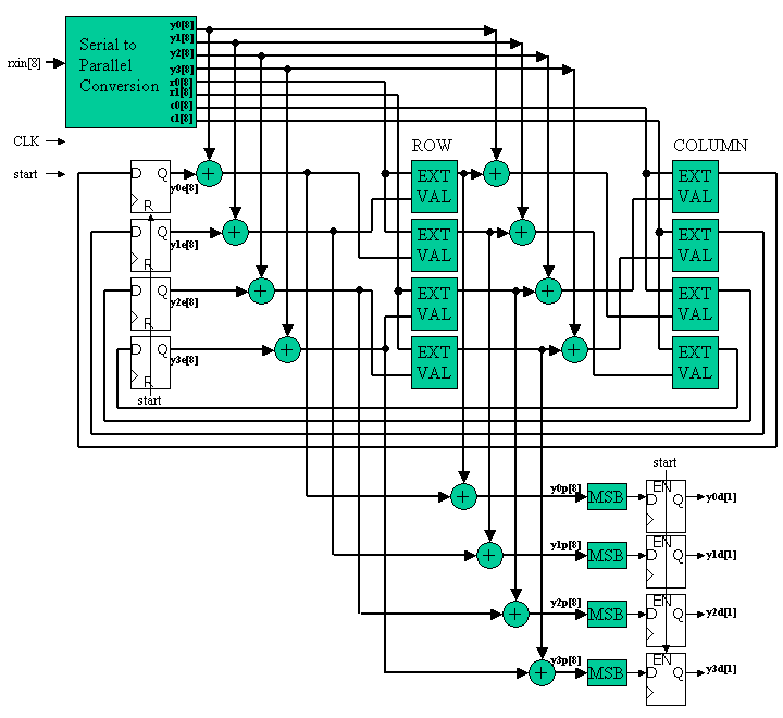
Figure 6 circuit design example
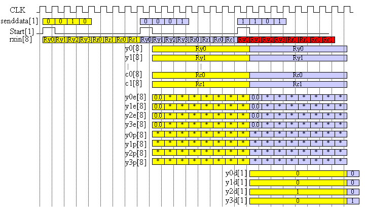
Figure 7 operating timing diagram
In this level of the task, you have to decode and output {y0d[1], y1d[1], y2d[1], y3d[1]} by using rxin and start.
And also you have to report how many bit error happened (fail in error correction) using the 10000 bit transmission data at the condition of SNR= 0dB, 3dB, 6dB, 9dB.
Table 1. Pin list for LEVEL1
|
2D DEC | |||
| Signal name | in or output | bit width | explanation |
| CLK | IN | 1 | system clock input |
| start | IN | 1 | assertion '1' indicates starting position |
| rxin | IN | 8 | transimission signal in two's complement |
| y0d | OUT | 1 | decoded out puts |
| y1d | OUT | 1 | |
| y2d | OUT | 1 | |
| y3d | OUT | 1 | |
20000 cycle rxin signal and start signal file is attached as follows. Code Rate R=1/2 then 20000 cycle means 10000 bit transmission.
For rxin 5 different noise is added. SNR= 0dB, 3dB, 6dB, 9dB and 100dB. 100dB means almost noise free for your debug.
Since rxin is two's complement 8 bit data, then it indicate -128 to 127 integer. Actual BPSK noise free wave anplitude is +32 or -32 is used.
Please report number of decoded bit errors for each SNR condition.
10000 bit transmitted information is also given as senddata.
start: start.txt
rxin (SNR=0dB, very big noise) : rxin0DB.txt
rxin (SNR=3dB, big noise) : rxin3DB.txt
rxin (SNR=6dB, middle level noise) : rxin6DB.txt
rxin (SNR=9dB, small noise) : rxin9DB.txt
rxin (SNR=9dB, no noise) :rxin100DB.txt
transimssion data 10000bits : senddata.txt
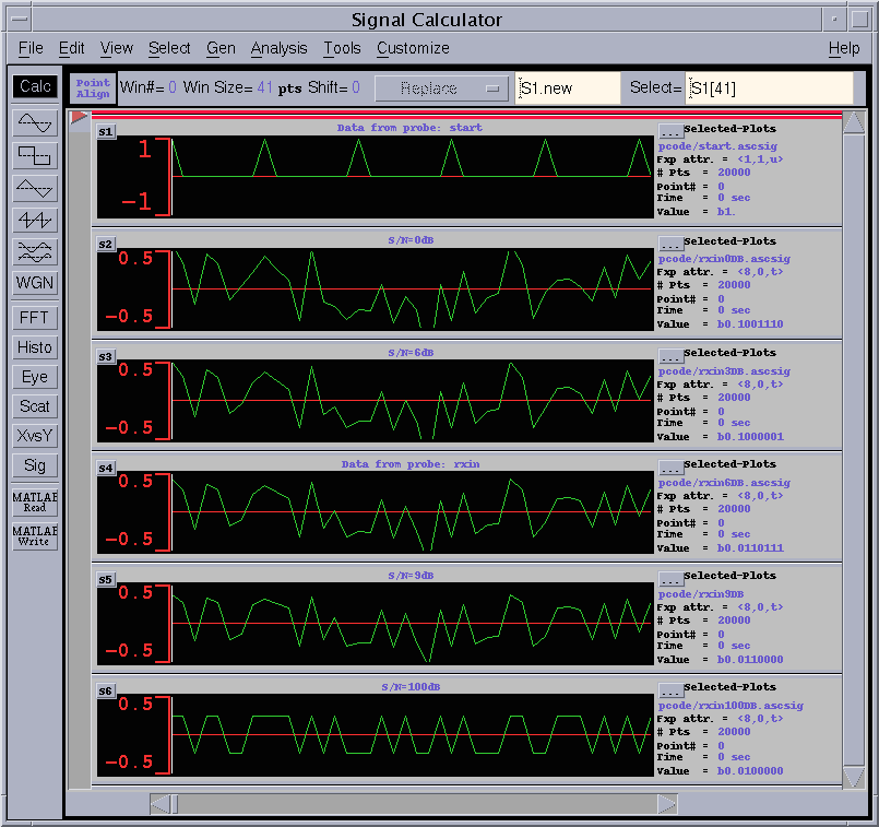
Figure 8 rxin wave for different SNR
Top wave in the figure 8 is start signal, then SNR=0, 3, 6, 9, 100dB from the next to the bottom.
In this wave viewer, the 8 bit signal is shifted to thr right by 7 bits. Then the BPSK level in the figure is 0.25 and -0.25.
Requirement is just decoding capability of this 20000 cycle data. You can freely change the specification.
Please report not only circuit clock cycle time and area, but also how many error bits for the different SNR should be reported.
Since it is impossible to use the same synthesis library for various participants,
In the previous example, total delay = 7.17 ns and 6 circuit stages, then the 7.17/6= 1.195 ns is the UNIT_DELAY of the speed. Please normalize your circuit speed by this UNIT_DELAY.
In the example, total cell area = 147.0 and 49 EXOR gates. Then 147.0/49=3.0 is the UNIT_AREA. Please normalize your circuit area by this UNIT_AREA.
| Title page | 1 | Team name, Members Name, School, Grade |
| 2 | Address, Phone, Email-address | |
| 3 | T-shirt size for all members in the team | |
| 4 | Which level of task is designed. | |
| Contents | 1 | Circuit block or architecture description |
| 2 | Designed circuit functional explanation, etc. | |
| 3 | Appealing point and originality | |
| 4 | Critical path speed, and circuit area, how many bit errors for each SNR | |
| 5 | HDL codes (VHDL or Verilog HDL) | |
| 6 | Simulation waveform indicating the design is operating! | |
| 7 | Anything you want to claim |
Report has to be emailed to the following address. Please use PDF file format.
If you want to send the report data other than PDF, please consult me.
This program is
operated by Univ. of Ryukyus, IE dept.,
co-operated by Okinawa Industry Support Center,
and co-sponsored by SONY LSI Design Inc and
Kyusyu Bureau of Economy, Trade and Industry.
ENJOY HDL! We want to see you at OKINAWA!